Printed Circuit Boards (PCBs) are the backbone of modern electronics, and ensuring their quality during assembly is critical to product reliability. From solder paste deposition to final testing, inspection plays a vital role in catching defects early, reducing rework, and improving yield. In this post, we’ll explore the various methods of PCB inspection used throughout the assembly process, highlighting their strengths, limitations, and ideal use cases.
Why PCB Inspection Matters
Defects in PCB assembly such as misaligned components, solder bridges, or insufficient solder, can lead to device failure, costly recalls, or safety hazards. Inspection ensures early defect detection, process control and optimization, compliance with quality standards and improved reliability and customer satisfaction.
Key Inspection Methods in PCB Assembly
- Solder Paste Inspection (SPI)
Stage: After solder paste printing
Purpose: Verifies the volume, height, and alignment of solder paste deposits.
Method:
- Uses 3D imaging or laser triangulation to measure paste deposits
- Detects issues like insufficient paste, bridging, or misalignment.
Benefits:
- Prevents soldering defects before component placement.
- Enables process feedback for stencil and printer adjustments.
- Automated Optical Inspection (AOI)
Stage: After component placement and post-reflow
Purpose: Detects visual defects such as missing components, tombstoning, solder bridges, and polarity errors.
Method:
- High-resolution cameras scan the board.
- Compares images to a golden reference using pattern recognition and algorithms.
Benefits:
- Fast and non-contact.
- Ideal for high-volume production.
- Can be used at multiple stages (pre-reflow and post-reflow).
Limitations:
- May struggle with hidden joints (e.g. BGAs).
- False positives can occur if programming isn’t optimized.
- X-Ray Inspection (AXI)
Stage: Post-reflow
Purpose: Inspects hidden solder joints and internal structures.
Method:
- Uses X-Rays to penetrate the board and visualize solder joints under components like BGAs, QFNs, and connectors.
Benefits:
- Reveals voids, cold joints, and bridging beneath opaque components.
- Essential for high-density and complex assemblies.
Limitations:
- Slower and more expensive than AOI.
- Requires skilled interpretation.
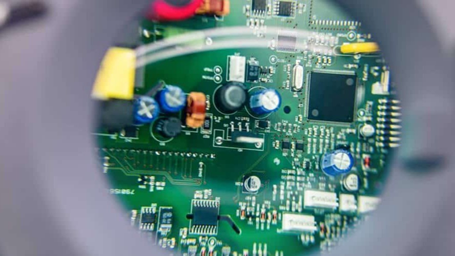
- Manual Visual Inspection
Stage: Throughout the process, especially for prototypes or low-volume runs
Purpose: Human inspection looking for obvious defects and anomalies.
Method:
- Technicians use magnifiers or microscopes to inspect boards.
Benefits:
- Flexible and intuitive
- Useful for small batches or unique boards.
Limitations:
- Subjective and inconsistent.
- Not scalable for high-volume production.
- Functional Testing (FCT)
Stage: Final Stage before shipping
Purpose: Verifies that the assembled PCB performs its intended function.
Method:
- Applies power and simulates real-world conditions.
- Measures outputs, voltages, currents, and communication protocols.
Benefits:
- Ensures end-to-end functionality.
- Catches issues that visual inspection can’t detect.
Limitations:
- Requires custom test fixtures and software.
- Time-consuming for complex boards.
- In-Circuit Testing (ICT)
Stage: After assembly, before final testing
Purpose: Tests individual components and connections on the PCB.
Method:
- Uses a bed-of-nails fixture to probe test points.
- Measures resistance, capacitance, and signal integrity.
Benefits:
- Fast and thorough for mass production.
- Detects shorts, opens, and component failures.
Limitations:
- Requires dedicated fixtures.
- Limited flexibility for design changes
If you’re still unsure of what inspection methods are right for your assembly, use the chart below as a guide. Note that testing methods may change while scaling production.
| Production Volume | Recommended Methods |
| Prototyping | Manual Inspection, AOI, Functional Testing |
| Low Volume | AOI, SPI, Manual Inspection |
| High Volume | SPI, AOI, AXI, ICT, Functional Testing |
| Complex Boards | AXI, AOI, Functional Testing |
In summary, PCB inspection isn’t just about catching defects. It’s about building a robust, repeatable process that ensures quality from start to finish. By combining multiple inspection methods, manufacturers like Janco Electronics, Inc. can create a layered defense against failure, optimize our assembly lines, and deliver reliable electronics to the market. Just as our customers expect us to.